| CPC H01J 37/32642 (2013.01) [H01J 37/32183 (2013.01); H01L 21/6833 (2013.01)] | 20 Claims |
|
1. A plasma processing apparatus comprising:
a plasma processing chamber;
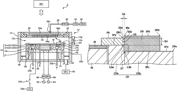
a substrate support disposed in the plasma processing chamber, the substrate support including a base and an electrostatic chuck disposed on the base;
at least one insulating ring disposed so as to surround the substrate support;
an inner conductive ring disposed on the electrostatic chuck and the at least one insulating ring so as to surround a substrate on the electrostatic chuck, the inner conductive ring having an outer side surface;
an outer conductive ring disposed on the at least one insulating ring so as to surround the inner conductive ring without contacting the inner conductive ring, the outer conductive ring having an inner side surface facing the outer side surface of the inner conductive ring;
a radio frequency power supply electrically coupled to the substrate support.
|