| CPC H01J 37/32449 (2013.01) [C23C 16/45565 (2013.01); C23C 16/52 (2013.01); H01J 37/32174 (2013.01); H01J 37/32559 (2013.01); H01J 37/32935 (2013.01)] | 15 Claims |
|
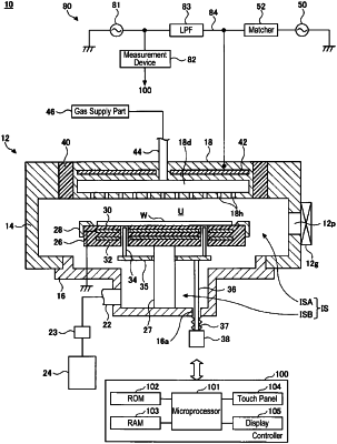
1. A plasma processing apparatus comprising:
a processing container;
a first electrode provided inside the processing container and connected to a high-frequency power supply;
a second electrode provided inside the processing container to face the first electrode, the second electrode being grounded; and
a film thickness calculator connected to at least one of the first electrode and the second electrode and configured to calculate a thickness of a film deposited on the at least one of the first electrode and the second electrode,
wherein the film thickness calculator is connected to the first electrode and is configured to calculate the thickness of the film deposited on a surface facing the second electrode in the first electrode, and
wherein the film thickness calculator is further configured to calculate the thickness of the film based on a current flowing in the first electrode when an AC voltage is applied to the first electrode.
|