| CPC H01J 37/3177 (2013.01) [H01J 37/045 (2013.01); H01J 2237/0437 (2013.01); H01J 2237/31776 (2013.01)] | 15 Claims |
|
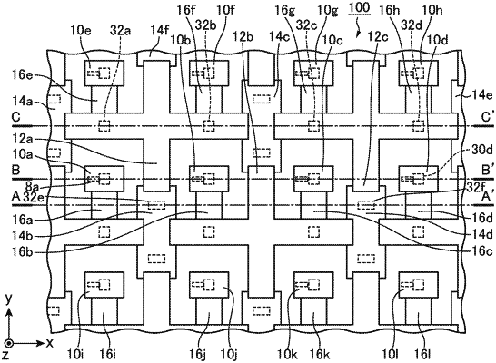
1. A semiconductor device comprising:
a substrate including a plurality of through holes provided at predetermined intervals along a first direction in a plane direction of the substrate and along a second direction intersecting the first direction in the substrate surface;
an insulating layer provided on the substrate, the insulating layer being penetrated by the through holes;
a plurality of first electrodes provided on the insulating layer, the first electrodes being adjacent to the respective through holes in the first direction;
a plurality of second electrodes provided on the insulating layer, the second electrodes being adjacent to the respective through holes in the first direction, the second electrodes being provided to face the first electrodes, the second electrodes being held at a predetermined potential; and
a wiring layer provided on the insulating layer, the wiring layer electrically connecting the adjacent second electrodes.
|