| CPC H01G 4/30 (2013.01) [H01G 4/008 (2013.01); H01G 4/012 (2013.01); H01G 4/1218 (2013.01)] | 13 Claims |
|
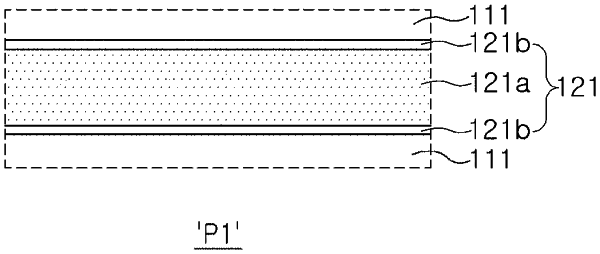
1. A multilayer electronic component comprising:
a body including dielectric layers and internal electrodes alternately disposed with the dielectric layers; and
external electrodes disposed on the body,
wherein one of the internal electrodes includes interfacial portions disposed at interfaces thereof with two of the dielectric layers, between which the one of the internal electrodes is disposed, and a central portion disposed between the interfacial portions, and
one of the interfacial portions has a Mn content higher than an average Mn content of the central portion and an average Mn content of one of the dielectric layers which is in contact with the one of the interfacial portions.
|