| CPC H01G 4/30 (2013.01) [C04B 35/468 (2013.01); H01G 4/008 (2013.01); H01G 4/012 (2013.01); H01G 4/1227 (2013.01); H01G 13/00 (2013.01); C04B 2235/66 (2013.01)] | 20 Claims |
|
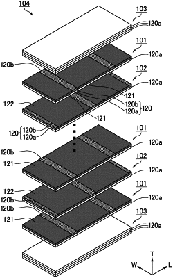
1. A method of manufacturing a multilayer ceramic capacitor comprising:
printing an internal electrode pattern on a dielectric layer;
forming a dielectric pattern in a region other than a region in which the internal electrode pattern is printed;
laminating a plurality of the dielectric layers to form a multilayer body;
exposing the internal electrode pattern and the dielectric pattern from a side surface of the multilayer body;
removing at least a portion of the exposed dielectric pattern; and
forming a dielectric gap layer on the side surface; wherein
the dielectric pattern includes a resin, and an amount of the resin included in the dielectric pattern is larger than an amount of a resin included in the internal electrode pattern.
|