| CPC H01G 4/30 (2013.01) [H01G 4/012 (2013.01); H01G 4/1227 (2013.01); H01G 4/248 (2013.01)] | 20 Claims |
|
1. A multilayer ceramic electronic component, comprising:
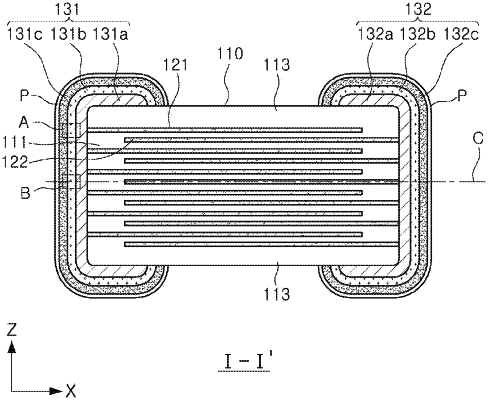
a ceramic body including a capacitance formation portion including a dielectric layer and first and second internal electrodes stacked in a stacking direction with the dielectric layer interposed therebetween, and including a first surface and a second surface opposing to each other in a first direction, a third surface and a fourth surface opposing to each other in a second direction, and a fifth surface and a sixth surface opposing to each other in a third direction which is the stacking direction; and
first and second external electrodes disposed on the first and second surfaces of the ceramic body, respectively, and including first and second base electrodes connected to the first and second internal electrodes and first and second conductive layers disposed to cover the first and second base electrodes, respectively,
wherein a ratio ‘b/a’ is more than 0.2 but less than 1, where a thickness of the first and second conductive layers in a respective central portion of the first and second surfaces of the ceramic body is ‘a’, and a thickness of the first and second conductive layers at a respective end of the capacitance formation portion is ‘b’,
wherein a total length of the multilayer ceramic electronic component in the first direction is less than 3.2 mm and equal to or greater than 1.6 mm, and
wherein entire portions of the first and second base electrodes respectively disposed on the first and second surfaces have a thickness in a range of 3 μm to 13 μm, and entire portions of the first and second conductive layers respectively disposed on the first and second surfaces have a thickness in a range of 3 μm to 13 μm.
|
|
11. A multilayer ceramic electronic component, comprising:
a ceramic body including a capacitance formation portion including a dielectric layer and first and second internal electrodes stacked in a stacking direction with the dielectric layer interposed therebetween, and including a first surface and a second surface opposing to each other in a first direction, a third surface and a fourth surface opposing to each other in a second direction, and a fifth surface and a sixth surface opposing to each other in a third direction which is the stacking direction; and
first and second external electrodes disposed on the first and second surfaces of the ceramic body, respectively, and including first and second base electrodes connected to the first and second internal electrodes and first and second conductive layers disposed to cover and being in direct physical contact with the first and second base electrodes, respectively,
wherein a ratio ‘b/a’ is more than 0.07 but less than 1, where a thickness of the first and second conductive layers in a respective central portion of the first and second surfaces of the ceramic body is ‘a’, and a thickness of the first and second conductive layers at a respective end of the capacitance formation portion is ‘b’,
wherein a total length of the multilayer ceramic electronic component in the first direction is 3.2 mm or more, and
wherein entire portions of the first and second base electrodes respectively disposed on the first and second surfaces have a thickness in a range of 3 μm to 13 μm, and entire portions of the first and second conductive layers respectively disposed on the first and second surfaces have a thickness in a range of 3 μm to 13 μm.
|