| CPC H01G 4/1209 (2013.01) [H01G 4/008 (2013.01); H01G 4/224 (2013.01)] | 20 Claims |
|
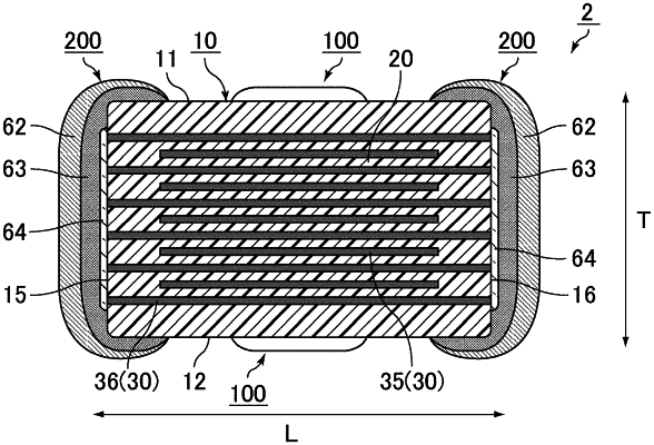
1. A method of producing a ceramic electronic component, comprising:
baking a first electrode paste containing a metal powder at a first temperature to form a first electrode layer at a first region of a ceramic body;
baking a second electrode paste containing a metal powder of a same type as the metal powder in the first electrode paste at a second temperature lower than the first temperature to form a second electrode layer at a second region different from the first region of the ceramic body; and
applying a physical shock treatment to a surface of the second electrode layer to densify a surface layer portion of the second electrode layer; wherein
the applying the physical shock treatment includes the physical shock treatment being applied to only the surface of the second electrode layer.
|