| CPC H01G 4/008 (2013.01) [H01G 4/012 (2013.01); H01G 4/232 (2013.01); H01G 4/30 (2013.01)] | 18 Claims |
|
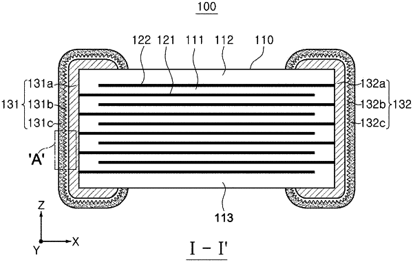
1. A multilayer electronic component comprising:
a body including a dielectric layer and an internal electrode; and
an external electrode including an electrode layer disposed on the body and connected to the internal electrode through a surface of the body, a first plating layer disposed on the electrode layer, and a conductive resin layer disposed on the first plating layer,
wherein the electrode layer includes Cu and glass, the first plating layer includes a Cu plating layer, and the conductive resin layer includes a conductive metal and a base resin, and
wherein the first plating layer has surface roughness at an interface with the conductive resin layer, and the first plating layer comprises an oxide containing Cu in a region having the surface roughness.
|