| CPC H01F 27/2804 (2013.01) [H01F 27/022 (2013.01); H01F 27/29 (2013.01); H01F 41/041 (2013.01); H01F 2027/2809 (2013.01)] | 20 Claims |
|
1. A coil electronic component, comprising:
a support substrate;
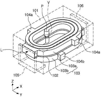
a coil pattern disposed on at least one surface of the support substrate;
a lead-out pattern disposed on at least one surface of the support substrate and connected to the coil pattern;
an encapsulant encapsulating at least portions of the support substrate, the coil pattern, and the lead-out pattern;
at least one protrusion protruding from one side surface of the coil pattern; and
an external electrode disposed on a mounting surface of the encapsulant and connected to the lead-out pattern,
wherein the lead-out pattern extends in a thickness direction of the support substrate to cover a side surface of the support substrate,
wherein the encapsulant includes an upper surface opposite the mounting surface in the thickness direction and a side surface connecting the mounting and upper surfaces, and
wherein the at least one protrusion is exposed to the side surface of the encapsulant and spaced apart from the mounting and upper surfaces in the thickness direction.
|