| CPC G11C 29/42 (2013.01) [G06F 11/1068 (2013.01); G11C 29/50004 (2013.01); G11C 2029/5004 (2013.01)] | 20 Claims |
|
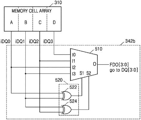
1. A memory device comprising:
a memory cell array comprising a plurality of memory cells, wherein the memory cell array is divided into multiple regions; and
a test controller configured to perform a parallel bit test (PBT) on the plurality of memory cells, wherein the test controller receives internal data from the multiple regions during the PBT, generates one or more select signals based on the internal data, generates fail data comprising a fail data bit indicating a region from the multiple regions based on the internal data and one or more select signals, and outputs the fail data via a data input/output signal line to the outside of the memory device.
|