| CPC G11C 11/4091 (2013.01) [G11C 11/4074 (2013.01); G11C 11/4087 (2013.01); G11C 11/40611 (2013.01); G11C 11/4076 (2013.01)] | 20 Claims |
|
1. An apparatus, comprising:
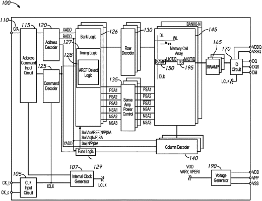
a command decoder circuit configured to provide an internal command signal;
a fuse logic circuit configured to store drive strength information and configured to provide a first plurality of drive strength control signals, a second plurality of drive strength control signals and a third plurality of drive strength control signals based on the drive strength information; and
a control circuit including:
a timing logic circuit configured to receive the internal command signal, configured to provide a first timing signal indicative of a threshold voltage compensation phase and a second timing signal indicative of a sense amplifier enable phase, and further configured to provide a selection signal responsive to the internal command signal;
a plurality of selectors configured to receive the second plurality of drive strength control signals and the third plurality of drive strength control signals, and further configured to provide either the second plurality of drive strength control signals or the third plurality of drive strength control signals responsive to the selection signal; and
a control signal generator circuit configured to receive the first timing signal, the second timing signal, the first plurality of drive strength control signals from the fuse logic circuit and either the second plurality of drive strength control signals or the third plurality of drive strength control signals from the plurality of selectors and further configured to provide a plurality of control signals,
wherein the control signal generator circuit is configured to provide the plurality of control signals based on the first plurality of drive strength control signals responsive to the first timing signals, and further configured to provide the plurality of control signals based on either the second plurality of drive strength control signals or the third plurality of drive strength control signals from the plurality of selectors responsive to the second timing signal.
|