| CPC G11C 11/4074 (2013.01) [G05F 1/575 (2013.01); G11C 5/147 (2013.01); G11C 7/14 (2013.01); G11C 11/4063 (2013.01); G11C 11/4091 (2013.01); H03H 7/06 (2013.01)] | 17 Claims |
|
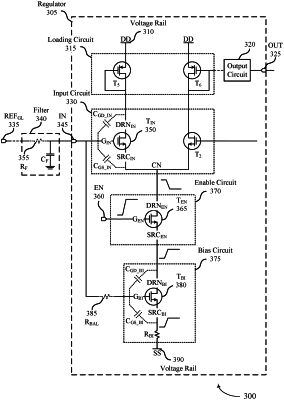
1. An apparatus, comprising:
a memory array comprising a plurality of memory sections;
a plurality of regulators coupled with the plurality of memory sections, wherein a regulator of the plurality of regulators comprises:
a first transistor coupled with an input node of the regulator, the first transistor configured to receive a reference signal via the input node;
a second transistor coupled with the input node, the second transistor configured receive the reference signal via the input node and to bias the regulator based at least in part on the reference signal, wherein a gate of the first transistor is coupled with a gate of the second transistor; and
a third transistor coupled with the first transistor via a first node, the second transistor via a second node, and an enable node of the regulator, the third transistor configured to receive an enable signal via the enable node and to enable an operation of the regulator based at least in part on the enable signal;
a signal generator configured to generate a global reference signal for the plurality of regulators; and
a plurality of low pass filters coupled with the plurality of regulators and the signal generator, wherein the plurality of low pass filters are configured to receive the global reference signal.
|