| CPC G11C 11/4074 (2013.01) [H01L 24/08 (2013.01); H01L 25/0657 (2013.01); H01L 2224/08145 (2013.01); H01L 2924/1436 (2013.01)] | 31 Claims |

|
1. A method comprising:
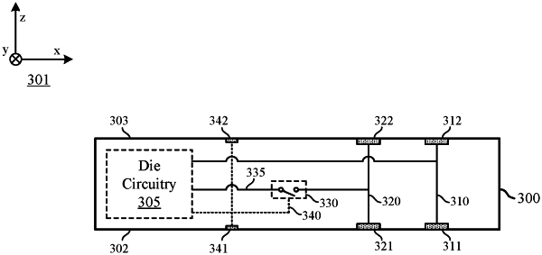
receiving a signal at a first semiconductor die, the first semiconductor die comprising circuitry associated with a first memory array and comprising a conductor coupling a power source with a second semiconductor die, the second semiconductor die comprising circuitry associated with a second memory array, wherein the signal comprises an indication of a condition of operating the circuitry associated with the second memory array; and
modifying, based at least in part on receiving the signal, a state of a switching component between the conductor and the circuitry associated with the first memory array.
|