| CPC G11C 11/40611 (2013.01) [G11C 7/1039 (2013.01); G11C 11/4085 (2013.01); G11C 11/4096 (2013.01); G11C 29/785 (2013.01)] | 18 Claims |
|
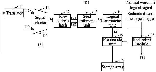
1. A refresh circuit, comprising:
a signal selector, configured to select one of a normal word line logical address and a redundant word line logical address as an output, an output signal of which is designated as a first logical address;
a row address latch, connected to an output terminal of the signal selector and configured to output a row hammer address and a row hammer flag signal according to the first logical address;
a seed arithmetic unit, connected to an output terminal of the row address latch and configured to receive a refresh signal as an excitation signal and generate a seed address according to the row hammer address;
a logical arithmetic unit, connected to an output terminal of the seed arithmetic unit and configured to obtain a row hammer refresh address according to the seed address, wherein the row hammer refresh address is an adjacent physical address of the seed address; and
a pre-decode unit, connected to an output terminal of the logical arithmetic unit and configured to receive the row hammer refresh address, and convert the row hammer refresh address into a physical address to be used by a memory array of a memory to perform a refresh operation.
|