| CPC G11C 11/2275 (2013.01) [G11C 11/2255 (2013.01); G11C 11/2257 (2013.01); G11C 11/2273 (2013.01); H10B 53/30 (2023.02)] | 6 Claims |
|
1. An oxide semiconductor-based FRAM, comprising:
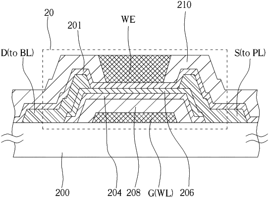
a substrate;
a word line on said substrate;
a gate insulating layer on said word line;
an oxide semiconductor layer on said gate insulating layer;
a source and a drain respectively on said oxide semiconductor layer and spaced apart at a distance, wherein said source and said drain further connect respectively to a plate line and a bit line;
a ferroelectric dielectric layer on said source, said drain and said oxide semiconductor layer; and
a write electrode on said ferroelectric dielectric layer, wherein said write electrode, said ferroelectric dielectric layer, said oxide semiconductor layer, said gate insulating layer and said word line overlap each other in a direction vertical to said substrate, wherein said write electrode, said ferroelectric dielectric layer and said oxide semiconductor layer constitute a ferroelectric capacitor, wherein a bias voltage and a reverse bias voltage are respectively applied on said write electrode and said plate line to write data in said ferroelectric capacitor.
|