US 11,721,370 B2
Semiconductor device
Tatsuya Onuki, Kanagawa (JP); Takanori Matsuzaki, Kanagawa (JP); Kiyoshi Kato, Kanagawa (JP); and Shunpei Yamazaki, Tokyo (JP)
Assigned to Semiconductor Energy Laboratory Co., Ltd.
Filed by Semiconductor Energy Laboratory Co., Ltd., Kanagawa-ken (JP)
Filed on Apr. 16, 2021, as Appl. No. 17/232,708.
Application 17/232,708 is a continuation of application No. 16/643,755, granted, now 10,984,840, previously published as PCT/IB2018/056697, filed on Sep. 3, 2018.
Claims priority of application No. 2017-170766 (JP), filed on Sep. 6, 2017; and application No. 2017-171116 (JP), filed on Sep. 6, 2017.
Prior Publication US 2021/0280221 A1, Sep. 9, 2021
This patent is subject to a terminal disclaimer.
Int. Cl. G11C 7/02 (2006.01); G11C 7/06 (2006.01); G11C 14/00 (2006.01)
CPC G11C 7/06 (2013.01) [G11C 14/0009 (2013.01)] 16 Claims
OG exemplary drawing
 
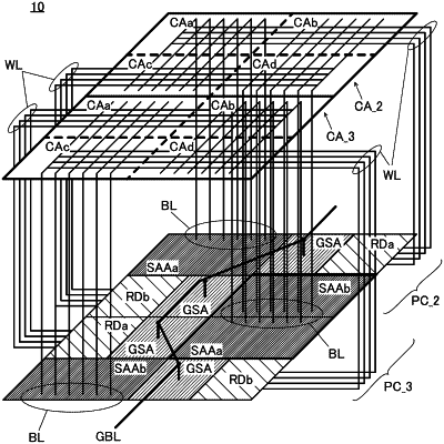
1. A semiconductor device comprising:
a cell array comprising a plurality of memory cells;
a driver circuit electrically connected to the cell array through a first wiring;
a first amplifier circuit electrically connected to the cell array through a second wiring; and
a second amplifier circuit electrically connected to the first amplifier circuit,
wherein the first amplifier circuit is configured to amplify a potential input from the cell array through the second wiring,
wherein the second amplifier circuit is configured to amplify a potential input from the first amplifier circuit, and
wherein each of the driver circuit, the first amplifier circuit, and the second amplifier circuit comprises a region overlapping with the cell array.