| CPC G09G 3/3258 (2013.01) [G06F 3/042 (2013.01); G06F 3/0421 (2013.01); G09G 2300/0439 (2013.01); G09G 2310/061 (2013.01); G09G 2320/0233 (2013.01); G09G 2360/14 (2013.01); G09G 2360/148 (2013.01); H04N 25/00 (2023.01); H04N 25/40 (2023.01); H04N 25/47 (2023.01)] | 20 Claims |
|
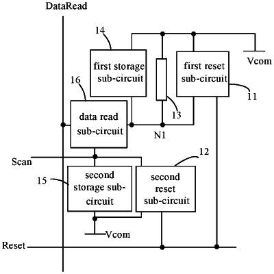
1. A photoelectric detection circuit, comprising: a first reset sub-circuit, a second reset sub-circuit, a first storage sub-circuit, a data read sub-circuit and a photosensitive device, wherein
a first terminal of the data read sub-circuit, a first terminal of the first storage sub-circuit, a first electrode of the photosensitive device and a first terminal of the first reset sub-circuit are connected to a first node; a second electrode of the photosensitive device is connected to a common voltage line;
the photosensitive device is configured to generate an inductive electrical signal based on a sensed light signal;
the data read sub-circuit is configured to transmit a voltage of the first node to a data read line in response to a signal of a scan line;
the first reset sub-circuit is configured to reset the voltage of the first node in response to a signal of a reset line;
the first storage sub-circuit is configured to store a voltage between the first node and the common voltage line; and
the second reset sub-circuit is configured to reset a voltage of the scan line in response to the signal of the reset line.
|