| CPC G09G 3/3258 (2013.01) [G09G 3/325 (2013.01); G09G 2300/0426 (2013.01); G09G 2300/0842 (2013.01); G09G 2310/0251 (2013.01); G09G 2310/061 (2013.01); G09G 2320/0233 (2013.01); G09G 2320/0247 (2013.01); H10K 59/12 (2023.02); H10K 59/1213 (2023.02)] | 25 Claims |
|
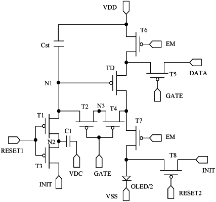
1. A pixel circuit, comprising:
a light emitting module configured to emit light;
a driving module configured to drive the light emitting module to emit light according to a driving voltage during a light emitting stage;
a storage module configured to maintain the driving voltage and to provide the driving voltage to the driving module during the light emitting stage;
a first transistor, a first electrode of the first transistor being connected to a position where the driving module receives the driving voltage, and a second electrode of the first transistor being not directly connected to a signal source;
a second transistor, a first electrode of the second transistor being connected to the first electrode of the first transistor, wherein a structure to which a second electrode of the second transistor is connected is different from a structure to which the second electrode of the first transistor is connected; wherein during the light emitting stage, a voltage at the second electrode of the first transistor is lower than that at the first electrode of the first transistor and a voltage at the second electrode of the second transistor is higher than that at the first electrode of the first transistor; and
a voltage stabilizing capacitor, a first electrode of the voltage stabilizing capacitor being connected to the second electrode of the first transistor, and a second electrode of the voltage stabilizing capacitor being connected to a constant voltage signal source.
|