| CPC G09G 3/3233 (2013.01) [H10K 59/131 (2023.02); G09G 2300/0819 (2013.01); G09G 2300/0842 (2013.01); G09G 2300/0861 (2013.01); G09G 2310/08 (2013.01)] | 18 Claims |

|
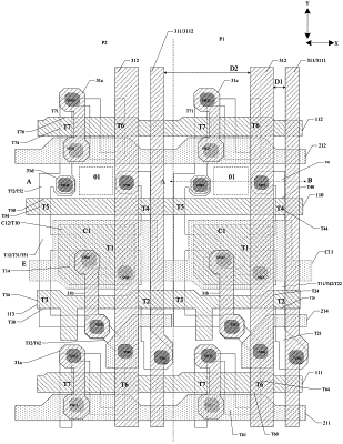
1. A display substrate, comprising:
a base substrate, comprising a display region;
a plurality of pixel units, located in the display region, each of the plurality of pixel units comprising a pixel circuit structure and a light-emitting element, the light-emitting element comprising a first electrode, the first electrode being located at a side of the pixel circuit structure away from the base substrate, the plurality of pixel units comprising a first pixel unit and a second pixel unit that are adjacent to each other in a first direction;
a first initialization signal line, extending in the first direction;
a light-emitting control signal line, extending in the first direction;
a first power line, extending in a second direction, the second direction intersecting with the first direction;
a first data line, extending in the second direction, the first data line being connected with the pixel circuit structure of the first pixel unit;
a second data line, extending in the second direction, the second data line being connected with the pixel circuit structure of the second pixel unit, the first data line and the second data line being arranged at two sides of the first power line, respectively; and
a light transmission hole, an orthographic projection of the light transmission hole on the base substrate being not overlapped with an orthographic projection of the first electrode on the base substrate,
wherein the light transmission hole is located in a region enclosed by the first initialization signal line, the light-emitting control signal line, the first power line, and the second data line.
|