| CPC G09G 3/3233 (2013.01) [G09G 2300/0819 (2013.01); G09G 2320/0214 (2013.01); G09G 2320/0233 (2013.01); G09G 2320/0238 (2013.01)] | 17 Claims |
|
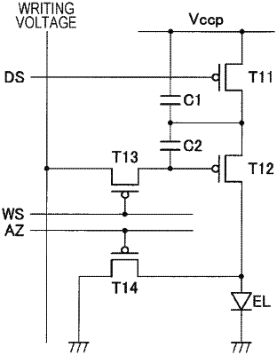
1. A pixel circuit comprising:
a light-emitting element;
a first capacitor, which is a metal insulator metal (MIM) capacitor;
a second capacitor, which is a metal oxide semiconductor (MOS) capacitor;
a sampling transistor configured to supply data voltage from a data line to the first capacitor; and
a driving transistor configured to supply, according to a voltage stored in the first capacitor, driving current from a first voltage line to the light-emitting element.
|