| CPC G09G 3/2092 (2013.01) [G09G 3/3266 (2013.01); G09G 2300/0408 (2013.01); G09G 2300/0426 (2013.01); G09G 2300/0809 (2013.01); G09G 2310/0286 (2013.01); G09G 2310/08 (2013.01); G11C 19/28 (2013.01); H10K 71/00 (2023.02)] | 23 Claims |
|
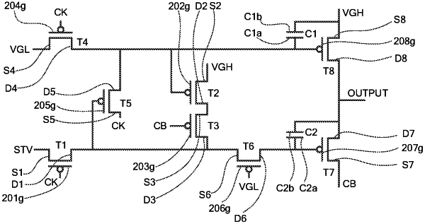
1. A display substrate, comprising: a substrate and a gate driving circuit provided on the substrate; the gate driving circuit includes: a frame start signal line, a clock signal line, an inverted clock signal line, a first level signal line, a second level signal line, and a plurality of shift register units, wherein
each of the plurality of shift register units includes a plurality of transistors, the plurality of transistors at least include a first transistor, a second transistor, and a third transistor, an active layer of the first transistor, an active layer of the second transistor and an active layer of the third transistor are formed by a continuous first semiconductor layer, the first semiconductor layer extends along a first direction; the first semiconductor layer includes at least three channel portions corresponding to the first transistor, the second transistor and the third transistor, and a conductive portion provided between adjacent channel portions, the at least three channel portions are arranged along the first direction, transistors corresponding to the adjacent channel portions are coupled to each other through a corresponding conductive portion;
the shift register unit includes a common connection terminal;
the plurality of transistors further include a fourth transistor and a fifth transistor, and an active layer of the fourth transistor and an active layer of the fifth transistor are formed by a continuous second semiconductor layer;
the active layer of the fourth transistor includes two fourth conductive portions arranged opposite to each other, and a fourth channel portion located between the two fourth conductive portions;
the active layer of the fifth transistor includes two fifth conductive portions arranged opposite to each other, and a fifth channel portion located between the two fifth conductive portions;
one of the fourth conductive portions and one of the fifth conductive portions are coupled to form a coupling end, and the coupling end is coupled to the common connection end through a first conductive connection portion.
|