| CPC G09G 3/20 (2013.01) [G02F 1/1343 (2013.01); H04N 7/144 (2013.01); H04N 23/54 (2023.01); H04N 23/55 (2023.01); G09G 2380/02 (2013.01)] | 20 Claims |

|
1. A display apparatus comprising:
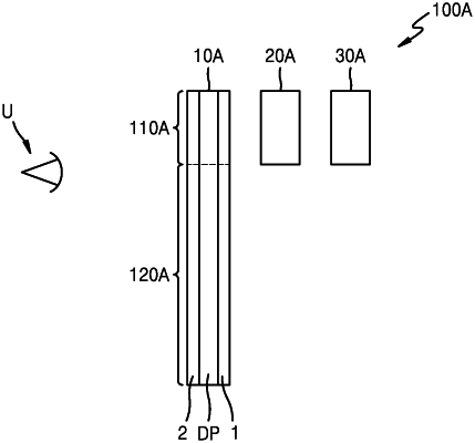
a display panel including a first display portion and a second display portion, the first display portion including a first emission device and a transmission area adjacent to the first emission device, and the second display portion including a second emission device and a non-emission area adjacent to the second emission device;
an electronic component facing one surface of the display panel and arranged to correspond to at least the transmission area of the first display portion; and
wherein each of the first emission device and the second emission device comprises:
a first electrode;
a second electrode facing the first electrode; and
an emission layer between the first electrode and the second electrode, and
wherein an insulating layer is disposed on the first electrodes of the first and second emission devices, the insulating layer including a first opening correspond to a part of the first electrode of the first emission device, a second opening corresponding to the transmission area of the first display portion and a third opening corresponding to a part of the first electrode of the second emission device, and the insulating layer disposed in the non-emission area in the second display portion.
|