| CPC G06V 40/1318 (2022.01) [H10K 59/126 (2023.02); H10K 59/1216 (2023.02); H10K 59/131 (2023.02); H10K 59/65 (2023.02)] | 18 Claims |

|
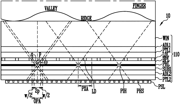
1. A fingerprint sensor for a display device comprising:
a substrate;
a light transmission layer including first openings in a first layer on the substrate and second openings in a second layer including circuit elements and wires;
a light emitting element layer on the light transmission layer and having at least one light emitting element that is electrically connected to at least one of the circuit elements and at least one of the wires; and
a sensor layer disposed on the substrate and having light sensors,
wherein:
at least a portion of the first openings and at least a portion of the second openings at least partially overlap;
the second openings have a closed shape formed by overlapping the at least one of the circuit elements and the at least one of the wires in a plan view;
the first openings are spaced apart from each other in the first layer;
the second openings are spaced apart from each other in the second layer;
the first openings and the second openings overlap each other in a one-to-one manner; and
the first openings and the second openings have widths or diameters between about 5 μm and about 20 μm.
|