| CPC G06V 10/7515 (2022.01) [G02B 27/017 (2013.01); G02B 27/0179 (2013.01); G06T 5/50 (2013.01); G06T 7/55 (2017.01); G02B 2027/0178 (2013.01); G02B 2027/0187 (2013.01)] | 20 Claims |
|
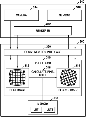
1. An electronic device comprising:
a communication interface; and
a processor configured to: receive, from an external device through the communication interface, a first image predistorted and rendered at a first time, calculate a pixel shift for each pixel of the received first image at a second time different from the first time, generate a second image by reprojecting the first image based on the calculated pixel shift, and transmit the generated second image to the external device through the communication interface.
|