| CPC G06F 13/4072 (2013.01) [G06F 13/1673 (2013.01)] | 20 Claims |
|
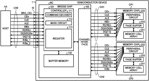
1. A semiconductor device comprising:
a terminal group configured to receive a plurality of signals from a host,
a first chip electrically connected to the terminal group and includes a first memory,
a plurality of second chips electrically connected to the first chip, the plurality of second chips being capable of outputting respective ready/busy signals; and
a plurality of first signal lines through which the ready/busy signals are respectively transferred from the second chips, wherein
each of the plurality of second chips is respectively connected to the first chip through a corresponding first signal line among the plurality of first signal lines, and wherein
the first chip is configured to:
receive the ready/busy signals from the plurality of second chips through the plurality of first signal lines,
store first information into the first memory, the first information containing states of the ready/busy signals of the second chips,
receive a first signal from the host through the terminal group, and
based on receiving the first signal from the host, output the first information stored in the first memory to the host.
|