US 11,720,485 B2
DRAM with command-differentiated storage of internally and externally sourced data
Thomas J. Sheffler, San Francisco, CA (US); Lawrence Lai, San Jose, CA (US); Liang Peng, San Jose, CA (US); and Bohuslav Rychlik, San Diego, CA (US)
Assigned to Rambus Inc., San Jose, CA (US)
Filed by Rambus Inc., San Jose, CA (US)
Filed on Apr. 25, 2022, as Appl. No. 17/728,791.
Application 17/728,791 is a continuation of application No. 17/540,437, filed on Dec. 2, 2021.
Application 17/540,437 is a continuation of application No. 16/735,303, filed on Jan. 6, 2020, granted, now 11,204,863, issued on Dec. 21, 2021.
Application 16/735,303 is a continuation of application No. 15/882,847, filed on Jan. 29, 2018, granted, now 10,552,310, issued on Feb. 4, 2020.
Application 15/882,847 is a continuation of application No. 15/497,126, filed on Apr. 25, 2017, granted, now 9,898,400, issued on Feb. 20, 2018.
Application 15/497,126 is a continuation of application No. 14/637,369, filed on Mar. 3, 2015, granted, now 9,658,953, issued on May 23, 2017.
Application 14/637,369 is a continuation of application No. 13/383,205, abandoned, previously published as PCT/US2010/039095, filed on Jun. 17, 2010.
Claims priority of provisional application 61/235,564, filed on Aug. 20, 2009.
Prior Publication US 2022/0253378 A1, Aug. 11, 2022
This patent is subject to a terminal disclaimer.
Int. Cl. G06F 12/02 (2006.01); G11C 7/22 (2006.01); G11C 8/10 (2006.01); G11C 7/10 (2006.01)
CPC G06F 12/023 (2013.01) [G11C 7/1006 (2013.01); G11C 7/1039 (2013.01); G11C 7/22 (2013.01); G11C 8/10 (2013.01); H05K 999/99 (2013.01); G06F 2212/2024 (2013.01); G11C 2207/107 (2013.01)] 20 Claims
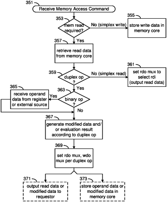
OG exemplary drawing
 
1. A dynamic random access memory (DRAM) device comprising:
a memory core having an array of DRAM cells;
a register to store first data in response to a register-write command;
a command/address interface that receives commands and addresses, the command/address interface to receive the register-write command and the first data, and then, after the first data has been stored in the register, to receive first and second memory access commands;
a data interface to receive second data in response to the second memory access command, wherein the data interface does not receive the first data; and
control circuitry to write the first data from the register to the memory core in response to the first memory access command and to write the second data from the data interface to the memory core in response to the second memory access command.