| CPC G06F 9/3001 (2013.01) [G06F 9/30029 (2013.01); G06F 9/30043 (2013.01); G06F 9/30189 (2013.01); G06F 9/3836 (2013.01); G06F 15/7821 (2013.01); H03K 19/20 (2013.01)] | 30 Claims |

|
1. A processing-in-memory (PIM) controller configured to control a PIM device having a memory function and an arithmetic function, the PIM controller comprising:
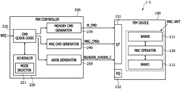
a read/arithmetic queue logic circuit configured to store a read queue for requesting to read out data stored in the PIM device and an arithmetic queue for requesting an arithmetic operation of the PIM device,
wherein the read/arithmetic queue logic circuit includes a read/arithmetic queue storage region having a plurality of read/arithmetic queue entries, each of which stores the read queue or the arithmetic queue;
wherein each of the plurality of read/arithmetic queue entries includes a flag;
wherein the flag of a read/arithmetic queue entry in which the read queue is stored among the plurality of read/arithmetic queue entries is set to have a first binary number;
wherein the flag of the read/arithmetic queue entry in which the arithmetic queue is stored among the plurality of read/arithmetic queue entries is set to have a second binary number; and
wherein the read/arithmetic queue logic circuit is configured to generate an arithmetic mode signal having a first level based on the flag that is set to have a second binary number, and configured to output the arithmetic queue from the read/arithmetic queue logic circuit in response to receiving an arithmetic mode enablement signal having the first level;
a write queue logic circuit configured to store a write queue for requesting to write data in the PIM device, configured to generate an arithmetic write signal having the first level when an arithmetic write queue used for execution of the arithmetic function exists in the write queue logic circuit, and configured to output the write queue from the write queue logic circuit in response to receiving an arithmetic write enablement signal having the first level; and
a scheduling logic circuit configured to perform a scheduling operation by adjusting an output sequence of the read queue, the arithmetic queue, and the write queue, configured to transmit the arithmetic mode enablement signal having the first level to the read/arithmetic queue logic circuit in response to receiving the arithmetic mode signal having the first level, and configured to transmit the arithmetic write enablement signal having the first level to the write queue logic circuit in response to receiving the arithmetic write signal having the first level.
|