| CPC G06F 3/0619 (2013.01) [G06F 3/0655 (2013.01); G06F 3/0673 (2013.01)] | 24 Claims |
|
1. An apparatus, comprising:
a memory array; and
a control component coupled with the memory array and configured to cause the apparatus to:
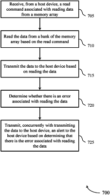
receive, from a host device, a read command associated with reading data from the memory array;
read the data from a bank of the memory array based at least in part on the read command;
transmit, to the host device concurrently with transmitting a first portion of the data to the host device and before transmitting a second portion of the data, an indication of an error status of the first portion of the data;
determine whether there is an error in a second portion of the data; and
transmit, after transmitting the indication of the error status and the first portion of the data and concurrently with transmitting the second portion of the data to the host device, an alert to the host device that there is the error in the second portion of the data.
|