| CPC G06F 3/0446 (2019.05) [G06F 1/1626 (2013.01); G06F 1/1637 (2013.01); G06F 1/1641 (2013.01); G06F 1/1643 (2013.01); G06F 1/1677 (2013.01); G06F 3/0412 (2013.01); G06F 3/1431 (2013.01); G06F 3/1446 (2013.01); G09G 2300/0426 (2013.01); G09G 2330/04 (2013.01); G09G 2340/0442 (2013.01); G09G 2354/00 (2013.01); G09G 2380/02 (2013.01)] | 8 Claims |
|
1. A foldable device comprising:
a first housing, a second housing, and a link between the first housing and the second housing; and
a flexible display panel including a display portion continuously provided over a top surface of the first housing, a top surface of the link, and a top surface of the second housing,
wherein when the foldable device is folded such that the top surface of the first housing faces the top surface of the second housing, part of the display portion which does not face a user of the foldable device is configured to stop display,
wherein the display portion comprises:
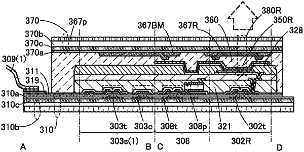
a first substrate having flexibility;
a first adhesive layer over the first substrate;
a transistor over the first adhesive layer;
an insulating layer over the transistor;
a lower electrode of a light-emitting element over the insulating layer;
a partition having a region overlapping with a first part of the lower electrode;
a layer containing a light-emitting organic compound, the layer overlapping with a second part of the lower electrode;
an upper electrode of the light-emitting element over the layer;
a photodiode below the light-emitting element;
a coloring layer over the upper electrode;
a second adhesive layer over the coloring layer; and
a second substrate having flexibility, and
wherein the photodiode is not overlapped with the light-emitting element and the coloring layer.
|