| CPC G06F 3/0443 (2019.05) [G06F 3/0412 (2013.01); G06F 3/0446 (2019.05); H01L 24/04 (2013.01); H01L 24/16 (2013.01); H01L 24/29 (2013.01); H01L 24/32 (2013.01); H01L 24/73 (2013.01); H01L 27/323 (2013.01); H01L 27/3223 (2013.01); H01L 27/3276 (2013.01); H01L 51/0097 (2013.01); H01L 51/5253 (2013.01); G06F 2203/04111 (2013.01); H01L 2224/0221 (2013.01); H01L 2224/02145 (2013.01); H01L 2224/04026 (2013.01); H01L 2224/16148 (2013.01); H01L 2224/29198 (2013.01); H01L 2224/32148 (2013.01); H01L 2224/73204 (2013.01); H01L 2924/1426 (2013.01)] | 20 Claims |
|
1. A display apparatus, comprising:
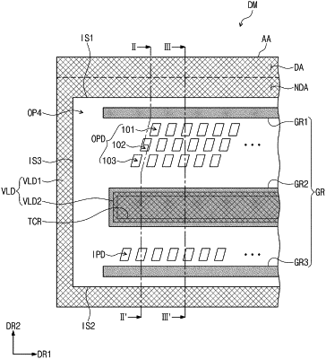
a display panel comprising a substrate comprising a display region and a non-display region adjacent to the display region, a first intermediate insulation layer which defines an opening overlapping the non-display region and disposed on the substrate, a pixel disposed in the display region, and a pad group connected to the pixel and overlapping the opening;
a driving circuit chip connected to the pad group and overlapping the opening; and
a touch sensor including a touch insulating layer disposed on the display panel and a touch electrode layer;
wherein the touch insulating layer comprises an intaglio pattern overlapping a portion of the driving circuit chip and passing through the touch insulating layer.
|
|
15. A display apparatus, comprising:
a display panel comprising a substrate comprising a display region and a non-display region adjacent to the display region, a pixel disposed in the display region, an output pad connected to the pixel, and an input pad spaced apart from the output pad;
a driving circuit chip connected to the output pad and input pad; and
a touch sensor including a touch insulating layer disposed on the display panel and a touch electrode layer;
wherein the touch insulating layer comprises at least one intaglio pattern disposed between the output pad and input pad.
|