| CPC G06F 3/0443 (2019.05) [G06F 3/0446 (2019.05); G06F 2203/04103 (2013.01); H10K 59/40 (2023.02); H10K 71/851 (2023.02)] | 7 Claims |
|
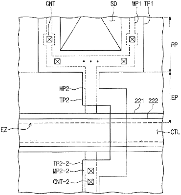
1. A method of fabricating a display device, the method comprising:
providing a display panel, in which a display region, a pad region, and a cutting region are defined, the pad region being adjacent to the display region and being located between the display region and the cutting region;
arranging an input sensor comprising a sensing pad, on the display panel; and
cutting the display panel and the input sensor along the cutting region,
wherein the arranging the input sensor comprises:
arranging a first pad, which is at least overlapped with the pad region and the cutting region, on the display panel;
arranging a second pad on the first pad; and
removing a portion of the first pad overlapped with the cutting region,
wherein the arranging the second pad is performed such that the second pad is not overlapped with the first pad in the cutting region.
|