| CPC G06F 3/0412 (2013.01) [G06F 3/0446 (2019.05); H10K 50/8426 (2023.02); H10K 59/131 (2023.02)] | 25 Claims |
|
1. A display device, comprising:
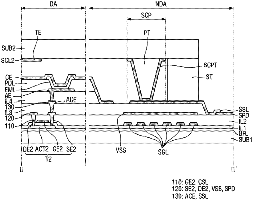
a first substrate including a display area and a non-display area;
a second substrate facing the first substrate;
a sealing member disposed in the non-display area and coupling the first substrate to the second substrate;
a sensing contact area disposed at an inner side of the sealing member;
a sensing signal line on the first substrate, the sensing signal line being disposed in the sensing contact area;
a sensing contact pattern on the second substrate, the sensing contact pattern being disposed in the sensing contact area and electrically connected to the sensing signal line;
a control signal line disposed between the first substrate and the sensing signal line;
a shielding pattern disposed between the control signal line and the sensing signal line, the shielding pattern overlapping the control signal line or the sensing signal line;
a first electrode on the first substrate;
a pixel defining layer on the first substrate and exposing at least a portion of the first electrode; and
a protrusion portion disposed in the sensing contact area and overlapping the sensing contact pattern,
wherein a thickness of the protrusion portion is greater than a thickness of the pixel defining layer.
|