| CPC G06F 3/0412 (2013.01) [G02F 1/13338 (2013.01); G06F 3/0443 (2019.05); G06F 3/04164 (2019.05); G06F 3/04184 (2019.05); G06F 3/041662 (2019.05); G06F 2203/04103 (2013.01)] | 10 Claims |
|
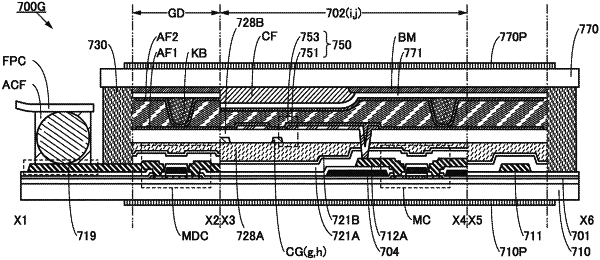
1. A display device comprising:
a signal line, a gate line, and a transistor over a substrate;
a first insulating film over the signal line, the gate line, and the transistor;
a first conductive film below the first insulating film;
a second conductive film over the first insulating film;
a pixel electrode of a display element, over the first insulating film;
a liquid crystal over the pixel electrode;
a second insulating film between the second conductive film and the pixel electrode; and
an alignment film below the liquid crystal,
wherein the transistor comprises:
a semiconductor film;
a gate electrode overlapping with the semiconductor film;
a gate insulating film between the semiconductor film and the gate electrode; and
a source electrode and a drain electrode in contact with the semiconductor film,
wherein the pixel electrode is electrically connected to one of the source electrode and the drain electrode through a first opening of the first insulating film,
wherein the pixel electrode is in contact with a top surface of the one of the source electrode and the drain electrode,
wherein the alignment film is positioned inside a second opening of the second insulating film,
wherein the first conductive film and the one of the source electrode and the drain electrode overlap each other,
wherein the first conductive film, the first opening, and the second opening overlap each other,
wherein the second conductive film has a function of an electrode of a touch sensor and a function of a common electrode of the display element, and
wherein each of the second conductive film and the pixel electrode has a slit.
|