| CPC G06F 3/0317 (2013.01) [G06F 3/03545 (2013.01); G06F 3/0412 (2013.01); H01L 25/167 (2013.01); H10K 50/86 (2023.02); H10K 59/122 (2023.02); H10K 59/40 (2023.02); G06F 3/044 (2013.01); G06F 3/04162 (2019.05); G06F 2203/04112 (2013.01); H10K 59/35 (2023.02); H10K 59/38 (2023.02)] | 19 Claims |
|
1. A display device comprising:
a thin-film transistor layer disposed on a substrate, the thin-film transistor layer including a thin-film transistor;
a light emitting element layer disposed on the thin-film transistor layer, the light emitting element layer including:
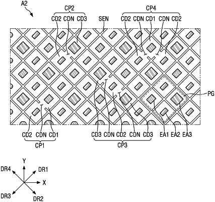
a pixel defining layer defining emission areas; and
a pixel electrode disposed in each of the emission areas;
a touch electrode disposed on the light emitting element layer, the touch electrode overlapping the pixel defining layer and sensing a touch; and
a code pattern defined by a planar shape of the pixel defining layer that is distinguished from the pixel electrode and the touch electrode, the code pattern having position information, wherein
the pixel defining layer absorbs light of a specific wavelength, and
the pixel electrode and the touch electrode reflect the light of the specific wavelength.
|