| CPC G05F 1/575 (2013.01) [G05F 1/461 (2013.01); H02M 1/15 (2013.01)] | 14 Claims |
|
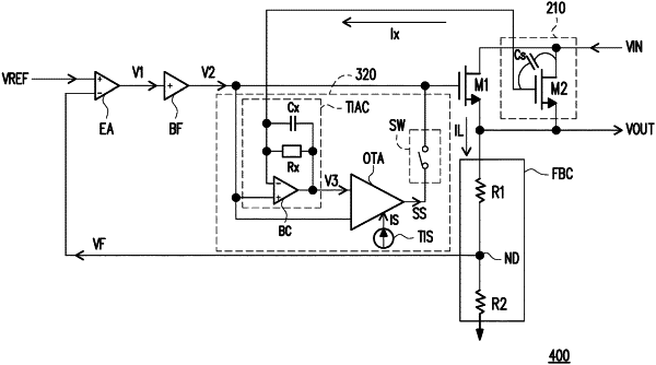
1. A voltage regulation circuit, comprising:
an error amplifier, configured to provide a control signal in response to a change in a feedback voltage, wherein a voltage value of the feedback voltage is related to a voltage value at an output terminal of the voltage regulation circuit;
an output transistor, a control terminal of the output transistor coupled to an output terminal of the error amplifier, and the output transistor configured to receive an input voltage signal and adjust an output voltage signal at the output terminal of the voltage regulation circuit in response to the control signal and the input voltage signal;
a noise extraction circuit, configured to extract a noise of the input voltage signal to provide a noise current signal; and
a stabilization circuit, coupled to the noise extraction circuit, and configured to convert the noise current signal into a stable signal and provide the stable signal to the control terminal of the output transistor in a high operating frequency range to cancel interference caused by the noise of the input voltage signal,
wherein the stabilization circuit comprises:
a first amplifier circuit, configured to convert the noise current signal into a conversion signal based on a first transfer function;
a second amplifier circuit, coupled to an output terminal of the first amplifier circuit, and configured to convert the conversion signal into the stable signal based on a second transfer function; and
a switch, coupled between an output terminal of the second amplifier circuit and the control terminal of the output transistor, and configured to:
be turned on in the high operating frequency range, so that the second amplifier circuit is coupled to the output transistor, and
be turned off in an operating frequency range outside the high operating frequency range, so that the second amplifier circuit is decoupled from the output transistor.
|