| CPC G03F 7/11 (2013.01) [C07D 209/48 (2013.01); C07D 403/14 (2013.01); C07D 487/04 (2013.01); C08F 26/06 (2013.01); C09D 139/04 (2013.01); G03F 7/094 (2013.01); H01L 21/0273 (2013.01); H01L 21/0337 (2013.01); H01L 21/76819 (2013.01)] | 20 Claims |
|
1. A material for forming an organic film, comprising:
a compound shown by the following general formula (1); and
X
 R1)n1 (1) R1)n1 (1)wherein X represents an organic group having a valency of n1 and 2 to 50 carbon atoms; n1 represents an integer of 1 to 10; and R1 represents at least one or more of the following general formulae (2) to (4),
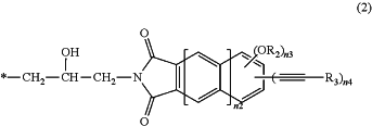 wherein an asterisk represents a bonding site to the organic group X; n2 represents 0 or 1; n3 and n4 represent integers satisfying relations of 0≤n3≤2, 0≤n4≤2, and 1≤n3+n4≤2; R2 represents any of a hydrogen atom, an allyl group, and a propargyl group; and R3 represents any of a hydrogen atom, a methyl group, and a phenyl group,
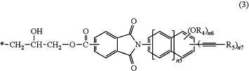 wherein an asterisk represents a bonding site to the organic group X; n5 represents 0 or 1; n6 and n7 represent integers satisfying relations of 0≤n6≤2, 0≤n7≤2, and 1≤n6+n7≤2; R4 represents any of a hydrogen atom, an allyl group, and a propargyl group; and R5 represents any of a hydrogen atom, a methyl group, and a phenyl group, and
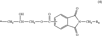 wherein an asterisk represents a bonding site to the organic group X; and R6 represents a monovalent organic group having an unsaturated bond and 1 to 10 carbon atoms.
|
|
6. A method for forming an organic film that serves as an organic flat film employed in a semiconductor device manufacturing process, the method comprising:
spin-coating a substrate to be processed with the material for forming an organic film according to claim 1; and
heating the substrate at a temperature of 100° C. or higher and 600° C. or lower for 10 seconds to 600 seconds to form a cured film.
|
|
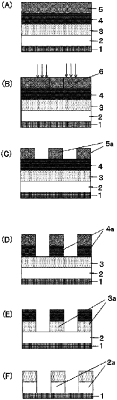
9. A patterning process comprising:
forming a resist underlayer film by using the material for forming an organic film according to claim 1 on a body to be processed;
forming a resist middle layer film by using a silicon-containing resist middle layer film material on the resist underlayer film;
forming a resist upper layer film by using a resist upper layer film material including a photoresist composition on the resist middle layer film;
forming a circuit pattern in the resist upper layer film;
etching the resist middle layer film while using the resist upper layer film having the formed pattern as a mask to transfer the pattern to the resist middle layer film;
etching the resist underlayer film while using the resist middle layer film having the transferred pattern as a mask to transfer the pattern to the resist underlayer film; and
further etching the body to be processed while using the resist underlayer film having the transferred pattern as a mask to form the pattern in the body to be processed.
|