| CPC G03F 7/0005 (2013.01) [G02B 25/001 (2013.01)] | 9 Claims |
|
1. A method, comprising:
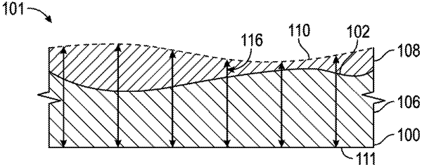
measuring a base substrate thickness distribution across a base substrate;
determining a target thickness change, the target thickness change determined by subtracting the base substrate thickness distribution from a target thickness distribution, the target thickness distribution corresponding to a thickness across one or more eyepiece areas of a substrate to be formed; and
forming a substrate having the target thickness distribution at the one or more eyepiece areas, the forming of the substrate having the target thickness distribution comprising:
disposing a resist over the base substrate and developing the resist utilizing a lithography process to form a gray-tone distribution having a thickness distribution corresponding to the target thickness distribution; or
disposing a resist over the base substrate with an inkjet printing process, the resist having a thickness distribution corresponding to the target thickness distribution and performing a transfer etch into the substrate, the transfer etch forming the target thickness distribution in the substrate.
|