| CPC G03F 1/32 (2013.01) [H01L 21/0337 (2013.01)] | 19 Claims |
|
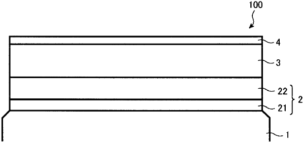
1. A mask blank comprising a phase shift film on a transparent substrate,
wherein a transmittance of the phase shift film with respect to an exposure light of a KrF excimer laser is 2% or more, and
wherein the phase shift film is configured to transmit the exposure light so that transmitted light has a phase difference of 150 degrees or more and 210 degrees or less with respect to the exposure light transmitted through the air for a same distance as a thickness of the phase shift film;
wherein the phase shift film has a structure where a lower layer and an upper layer are stacked in order from a side of the transparent substrate;
wherein a refractive index nL of the lower layer at a wavelength of the exposure light and a refractive index nU of the upper layer at a wavelength of the exposure light satisfy a relation of nL>nU;
wherein an extinction coefficient kL of the lower layer at a wavelength of the exposure light and an extinction coefficient kU of the upper layer at a wavelength of the exposure light satisfy a relation of kL>kU; and
wherein a thickness dL of the lower layer and a thickness dU of the upper layer satisfy a relation of dL<dU.
|