| CPC G02F 1/157 (2013.01) [G02F 1/1533 (2013.01); H10K 59/124 (2023.02); H10K 59/50 (2023.02)] | 11 Claims |
|
1. A display panel, wherein the display panel comprises:
a plurality of displaying regions, each of the plurality of displaying regions comprising a plurality of pixel points; and
a plurality of light transmission regions, wherein each of the plurality of light transmission regions is disposed adjacent to one of the plurality of displaying regions, and comprises light transmission thin films laminated;
wherein each of the plurality of light transmission regions further comprises a light transmittance adjustment layer disposed between any adjacent two of the plurality of light transmission thin films;
wherein the plurality of displaying regions and the plurality of light transmission regions are disposed alternately;
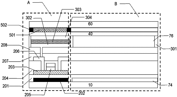
wherein each of the plurality of displaying regions comprises: a substrate; a thin film transistor layer, the thin film transistor layer located on the substrate; a light emitting layer, the light emitting layer located on the thin film transistor layer; and a color filter layer, the color filter layer located on the light emitting layer;
wherein the thin film transistor layer comprises transparent insulation layers laminated, the light transmission thin films comprise extension portions of the transparent insulation layers extending toward an outside of the thin film transistor layer;
wherein the light transmittance adjustment layer is located on the light emitting layer, and is disposed alternately with the color filter layer;
wherein a bottom surface of the color filter layer is coplanar with a bottom surface of the light transmittance adjustment layer;
wherein the light transmission thin films comprise a buffer layer, an interlayer dielectric layer, a first planarization layer, and a second planarization layer; and
wherein an auxiliary light modulating layer is located in the buffer layer and overlaps with the light transmittance adjustment layer in a plan view, a side wall of the auxiliary light modulating layer is coplanar with a sidewall of the light transmittance adjustment layer.
|