| CPC G02F 1/1368 (2013.01) [G02F 1/136209 (2013.01); G02F 1/136286 (2013.01)] | 12 Claims |

|
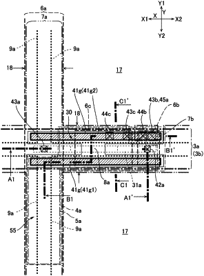
1. An electro-optical device, comprising:
a substrate body;
a transistor including a semiconductor layer including a first source drain region, a channel region, and a second source drain region;
a first interlayer insulating layer provided in a layer between the substrate body and the semiconductor layer;
a light shielding layer overlapping in plan view with the semiconductor layer in a layer between the substrate body and the first interlayer insulating layer;
a first light shielding wall penetrating the first interlayer insulating layer so as to reach the light shielding layer through a side of the semiconductor layer;
a second light shielding wall penetrating the first interlayer insulating layer so as to reach the light shielding layer on a side of the semiconductor layer opposite to the first light shielding wall;
a second interlayer insulating layer configured to cover the transistor from a side opposite to the substrate body;
a first data line; and
a second data line adjacent to the first data line, wherein
an entirety of the semiconductor layer has a constant width along an extension direction of the semiconductor layer,
the second interlayer insulating layer is provided with a first contact hole extending through the second interlayer insulating layer to reach the first source drain region,
a width of the first source drain region is the same as a width of a first opening portion of the first contact hole that opens on a side of the first source drain region, or is less than the width of the first opening portion,
the first source drain region includes a first contact region and a first low concentration region provided between the first contact region and the channel region,
the second source drain region includes a second contact region and a second low concentration region provided between the second contact region and the channel region,
the first contact region overlaps with the first data line in plan view,
the first low concentration region, the channel region, the second low concentration region, and the second contact region are provided between the first data line and the second data line in plan view,
the first light shielding wall and the second light shielding wall extend from a side of the first contact region to a side of the second contact region, and
a part of the first light shielding wall and a part of the second light shielding wall overlap with the first data line in plan view.
|