| CPC G02F 1/136286 (2013.01) [G02F 1/1368 (2013.01); G02F 1/133512 (2013.01); G02F 1/134309 (2013.01); G02F 1/133514 (2013.01); G02F 1/133707 (2013.01); G02F 1/134372 (2021.01); G02F 2201/40 (2013.01); H01L 27/124 (2013.01)] | 20 Claims |
|
1. A transistor substrate, comprising:
a plurality of data lines; and
a plurality of scan lines intersecting with the plurality of data lines to define a plurality of pixel units, wherein one of the plurality of pixel units comprises:
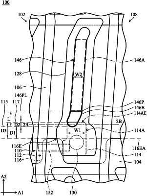
a first electrode having a slit, wherein the slit comprises a major axis portion and a curved portion connected to the major axis portion;
a second electrode, wherein one of the first electrode and the second electrode is used for receiving a pixel voltage signal, and the other one of the first electrode and the second electrode is used for receiving a common voltage signal; and
a switching transistor comprising a switching electrode;
wherein the switching electrode and the curved portion of the slit have an overlapping region, and an area of the overlapping region is 0.2 times to 0.8 times an area of the curved portion.
|