| CPC G02F 1/1347 (2013.01) [G02F 1/13394 (2013.01); G02F 1/13396 (2021.01); G02F 1/13398 (2021.01); G02F 1/13471 (2013.01); G02F 1/133512 (2013.01); G02F 1/133514 (2013.01); G02F 1/133528 (2013.01); G02F 1/133617 (2013.01); G02F 1/134309 (2013.01); G02F 1/136286 (2013.01); G02F 1/133548 (2021.01); G02F 1/133614 (2021.01); G02F 2201/121 (2013.01); G02F 2201/123 (2013.01)] | 18 Claims |
|
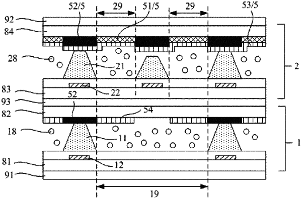
1. A display panel, comprising:
a first sub-panel, comprising a first substrate and a second substrate opposite to each other, and a first medium and a first spacer wall between the first substrate and the second substrate, wherein the first sub-panel has a plurality of filter pixels which are arranged at intervals, and the filter pixels are configured to generate a driving electric field to control light transmittance of the first medium; the first spacer wall is black and is arranged along spaces between the plurality of filter pixels, and a dielectric coefficient of the first spacer wall is greater than a dielectric coefficient of the first medium; and
a second sub-panel on a light emergent side of the first sub-panel and comprising a third substrate and a fourth substrate opposite to each other, and a second medium and a second spacer wall between the third substrate and the fourth substrate, wherein the second sub-panel has a plurality of display pixels which are arranged at intervals, and the display pixels are configured to generate a driving electric field to control light transmittance of the second medium; the second spacer wall is black and is arranged along spaces between the plurality of display pixels, and a dielectric coefficient of the second spacer wall is greater than a dielectric coefficient of the second medium,
wherein the second substrate is closer to the second sub-panel than the first substrate, the third substrate is closer to the first sub-panel than the fourth substrate, the first spacer wall is disposed on the first substrate at a side of the first substrate facing the second substrate, the second spacer wall is disposed on the third substrate at a side of the third substrate facing the fourth substrate, and an orientation of the first spacer wall is the same as an orientation of the second spacer wall,
a size of the first spacer wall decreases along a direction pointing from the first substrate to the second substrate, and a size of the second spacer wall decreases along a direction pointing from the third substrate to the fourth substrate,
at least part of the filter pixels comprise an auxiliary fluorescence conversion structure, an orthographic projection of the at least part of the filter pixels on the fourth substrate covers orthographic projections of at least two of the display pixels on the fourth substrate, an orthographic projection of the auxiliary fluorescence conversion structure on the fourth substrate completely coincides with the orthographic projections of the at least two of the display pixels on the fourth substrate, and the auxiliary fluorescence conversion structure is configured to convert light of a wavelength shorter than a wavelength of light of a color of the display pixel aligned with the auxiliary fluorescence conversion structure into light of the color of the display pixel.
|