| CPC G02F 1/134309 (2013.01) [G02F 1/1368 (2013.01); G06F 1/3265 (2013.01); G06F 3/044 (2013.01); G06F 3/0446 (2019.05); G02F 1/134345 (2021.01); G02F 1/134372 (2021.01); G02F 1/136286 (2013.01); G02F 2201/121 (2013.01); G02F 2201/123 (2013.01); G02F 2201/40 (2013.01); Y02D 10/00 (2018.01)] | 11 Claims |
|
1. A display device comprising a pixel,
wherein the pixel comprises a plurality of subpixels,
wherein each of the subpixels comprises a display region,
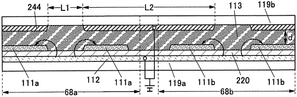
wherein the display device comprises, a first common electrode, a second common electrode, a pixel electrode, an auxiliary wiring, and a liquid crystal layer,
wherein the second common electrode overlaps with the first common electrode and the pixel electrode,
wherein the second common electrode includes an opening in the display region of the subpixel,
wherein in a cross-sectional view of the display device, the opening of the second common electrode overlaps with a region which is not provided with the pixel electrode,
wherein at least either of the first common electrode or the pixel electrode does not overlap with the opening,
wherein the auxiliary wiring is in contact with the first common electrode,
wherein, when a thickness of the liquid crystal layer is denoted by d, a width of the opening is greater than or equal to d/2 and narrower than a width of the subpixel,
wherein, when a thickness of the liquid crystal layer is denoted by d, a distance between the openings of two adjacent subpixels is greater than or equal to 1.2d and less than or equal to 2.4d, and
wherein a thickness of the liquid crystal layer is greater than or equal to 1.5 μm and less than or equal to 3 μm.
|