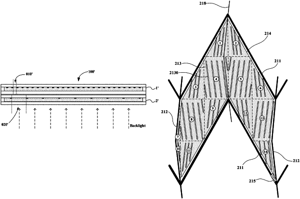
| CPC G02F 1/133707 (2013.01) [G02F 1/1368 (2013.01); G02F 1/134336 (2013.01); G02F 1/136286 (2013.01)] | 18 Claims |

|
1. An array substrate comprising:
a first transparent electrode layer with a plurality of slit structures, wherein the first transparent electrode layer comprises a plurality of domains, the plurality of domains comprise at least two types of domains, each of the plurality of domains is adjacent to different types of domains along both a row direction and a column direction, slit structures located in a same type of domain extend in a same direction, and slit structures located in different types of domains extend in different directions; and
a plurality of gate lines extending along the row direction and a plurality of data lines extending along the column direction, the plurality of gate lines and the plurality of data lines crossing to define a plurality of dimming regions arranged in an array, wherein each of the plurality of dimming regions is overlapped with the at least two types of domains in the first transparent electrode layer,
wherein:
each of the plurality of gate lines extends in a fold-line waveform along the row direction, and comprises a plurality of first fold line units arranged periodically, wherein each of the plurality of first fold line units comprises two first straight line segments symmetrically arranged with the column direction as a symmetry axis;
each of the plurality of data lines extends in a fold-line waveform along the column direction and comprises a plurality of second fold line units arranged periodically, wherein each of the plurality of second fold line units comprises a first subsegment and a second subsegment which are centrosymmetric, and the first subsegment and the second subsegment each comprise two second straight line segments symmetrically arranged with the row direction as a symmetric axis; and
the array substrate further comprises: a common electrode line located between adjacent two of the plurality of data lines, wherein the common electrode line extends in a fold-line waveform along the column direction and comprises a plurality of third fold line units arranged periodically, each of the plurality of third fold line units comprises a third subsegment and a fourth subsegment which are centrosymmetric, and the third subsegment and the fourth subsegment each comprise two third straight line segments symmetrically arranged with the row direction as a symmetric axis.
|