| CPC G02F 1/1309 (2013.01) [G01N 23/2251 (2013.01); G01N 27/205 (2013.01); H01L 22/14 (2013.01); H01L 22/32 (2013.01); H01L 22/34 (2013.01)] | 13 Claims |
|
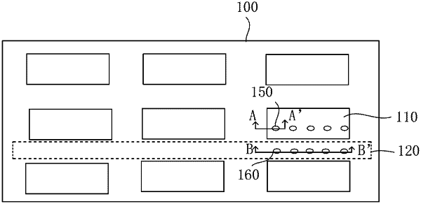
1. A substrate, divided into at least one display substrate area and an interval area located between the at least one display substrate area, wherein the interval area is provided with at least one test area, the substrate comprising:
a sub stratum;
a metal layer disposed on the substratum;
an insulating layer disposed on the metal layer;
a plurality of first via holes disposed in the display substrate area and passing through the insulating layer of the display substrate area;
at least one second via hole disposed in the at least one test area and passing through the insulating layer of the at least one test area;
a plurality of first transparent electrodes disposed on the insulating layer of the display substrate area and in the plurality of first via holes and connected with the metal layer; and
a plurality of second transparent electrodes disposed in the at least one second via hole and connected with the metal layer;
wherein the plurality of first via holes and the at least second via hole are formed through the same manufacture procedure, and the plurality of first transparent electrodes and the plurality of second transparent electrodes are formed through the same manufacture procedure;
wherein the substrate comprises more than one second via hole and further comprises at least one conductor, wherein each of the at least one conductor is connected with at least two of the plurality of second transparent electrodes corresponding to the second via holes; and wherein the at least one conductor and the corresponding connected second transparent electrodes form a test circuit;
wherein the substrate further comprises at least two pads, wherein the at least two pads are disposed at both ends of the test circuit and are connected with the second transparent electrodes or the at least one conductor;
wherein the at least two pads and the metal layer are formed through the same manufacture procedure, and the at least two pads are not connected with the metal layer; and
the insulating layer is provided with a through hole at a position corresponding to each of the at least two pads, and the plurality of second transparent electrodes are connected with the at least two pads through the respective through holes.
|