| CPC G02F 1/0356 (2013.01) [G02F 1/212 (2021.01); G02F 1/2255 (2013.01)] | 6 Claims |
|
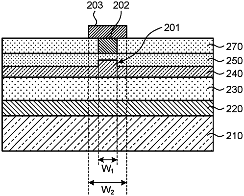
1. An optical device comprising:
a ground electrode having a ground potential;
a thin film optical waveguide formed by a thin film substrate stacked on the ground electrode;
a dielectric layer that is stacked on the thin film substrate, the position where the dielectric layer is in alignment with the thin film optical waveguide being formed into an opening;
a signal electrode embedded in the opening and that transmits a high frequency signal,
wherein a side surface of the signal electrode is covered with the dielectric layer, while a top surface of the signal electrode is exposed.
|