| CPC G02F 1/0107 (2013.01) [G02F 1/1303 (2013.01); G02F 1/1339 (2013.01); G02F 1/1341 (2013.01); G02F 1/13394 (2013.01); G02F 1/133509 (2013.01); G02F 1/133512 (2013.01); G02F 1/133514 (2013.01); G02F 1/134309 (2013.01); G02F 1/13312 (2021.01); G02F 1/13398 (2021.01); G02F 1/133322 (2021.01); G02F 1/133325 (2021.01); G02F 1/133388 (2021.01)] | 10 Claims |
|
1. A display device comprising:
a first insulating substrate including a first area and a second area which is disposed outside of the first area,
a pixel on the first insulating substrate, in the first area,
a signal wiring through which a signal for driving the pixel is transmitted, the signal wiring in the first area, on the first insulating substrate and disposed a distance from the first insulating substrate,
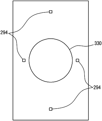
a hole which is disposed in the second area and has a depth which extends into a thickness of the first insulating substrate,
a first dummy wire and a second dummy wire which are disposed in the second area, disposed on the first insulating substrate, disconnected from each other along the second area, and disposed a distance from the first insulating substrate, and
in sequential order along the first insulating substrate, the first dummy wire, the hole and the second dummy wire,
wherein the first dummy wire and the second dummy wire are spaced from a center of the hole by a same distance.
|