| CPC G02B 7/34 (2013.01) [G03B 13/36 (2013.01); H04N 23/61 (2023.01); H04N 23/631 (2023.01); H04N 23/67 (2023.01); H04N 23/672 (2023.01); H04N 23/675 (2023.01); H04N 25/445 (2023.01); H04N 25/702 (2023.01); H04N 25/704 (2023.01); H04N 25/77 (2023.01); H04N 25/778 (2023.01); H04N 23/611 (2023.01)] | 14 Claims |
|
1. An image sensor comprising:
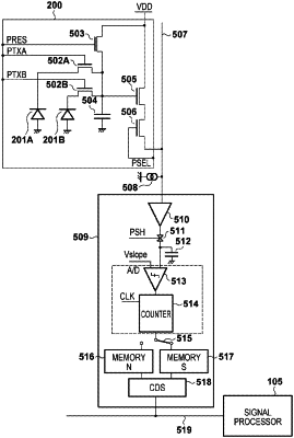
a pixel portion in which a plurality of unit pixels each having one micro lens and a plurality of photoelectric conversion portions are arrayed in a matrix;
a signal holding portion configured to hold signals corresponding to electric charges accumulated in a part of the photoelectric conversion portions among the plurality of photoelectric conversion portions in each of the unit pixels and signals corresponding to electric charges obtained by combining electric charges accumulated in all of the photoelectric conversion portions in each of the unit pixels;
an output portion configured to output signals based on the signals corresponding to electric charges accumulated in the part of the photoelectric conversion portions among the plurality of photoelectric conversion portions in each of the unit pixels and signals based on signals corresponding to electric charges obtained by combining electric charges accumulated in all of the photoelectric conversion portions in each of the unit pixels, the signals being held in the holding portion,
wherein the pixel portion is formed on a first semiconductor substrate and the signal holding portion is formed on a second semiconductor substrate different from the first semiconductor substrate, and
wherein the first semiconductor substrate and the second semiconductor substrate are stacked with each other.
|