| CPC G02B 6/4268 (2013.01) [G02B 6/4214 (2013.01); G02B 6/4204 (2013.01); G02B 6/4272 (2013.01); H01L 2224/16225 (2013.01); H01L 2924/15192 (2013.01); H01L 2924/15311 (2013.01)] | 20 Claims |
|
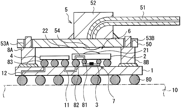
1. An optical transmission module comprising:
a first substrate having a surface;
a driving circuit disposed over the surface of the first substrate;
one or more wirings disposed in contact with the first substrate;
an optical element having a first surface and a second surface and including a light emitting element, the second surface of the optical element disposed over the one or more wirings along a plane that is transverse to the second surface of the optical element, and the optical element is electrically connected to the driving circuit via the one or more wirings;
a second substrate having a first surface and a second surface;
a lens disposed on the first surface of the second substrate; and
a connection member that connects together the first surface of the second substrate and the surface of the first substrate,
wherein the first surface of the second substrate is separated from the second surface of the optical element by a predetermined distance.
|