| CPC G02B 5/3083 (2013.01) [G02B 5/003 (2013.01); H04M 1/0264 (2013.01); H04M 1/0266 (2013.01)] | 11 Claims |
|
1. A method of manufacturing an electronic device, the method comprising the steps of:
providing a display panel;
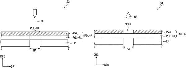
providing a polarizer including a polarizer layer at an outermost layer thereof on the display panel;
irradiating a laser beam onto a portion of the polarizer layer; and
providing a substantially neutral solution having a temperature from about 5° C. to about 40° C. onto the portion of the polarizer layer irradiated with the laser beam,
wherein the polarizer layer comprises an elongated film and a light-absorbing material adsorbed to the elongated film, the step of irradiating of the laser beam comprises detaching the light-absorbing material by the laser beam, and the step of providing of the neutral solution comprises extracting the detached light-absorbing material by the neutral solution.
|